


Usage of Different Grades of Chips
(This is an article generated by ChatGPT)
Semiconductor chips are manufactured at different process nodes (measured in nanometers, or nm), which refer to the size of the smallest features on a chip. The smaller the process node, the more transistors can be packed onto a chip, improving performance, power efficiency, and density. However, larger process nodes (older technologies) still play a critical role in industries that prioritize cost, reliability, and lower power consumption over sheer computing power.
1. Understanding Process Nodes: What Does 3nm, 5nm, 30nm Mean?
The "nm" (nanometer) number does not directly represent transistor size, but rather serves as a marketing term for transistor density and improvements in power efficiency. Generally:
Smaller nodes (e.g., 3nm, 5nm, 7nm) → Used for cutting-edge computing, AI, and high-performance applications.
Mid-range nodes (e.g., 14nm, 22nm, 30nm) → Used for mainstream processors, industrial applications, and automotive electronics.
Larger nodes (e.g., 45nm, 65nm, 90nm, 180nm, 250nm) → Used in cost-sensitive applications, sensors, analog circuits, and mature embedded systems.
2. Breakdown of Process Node Usage by Industry and Application
(A) Cutting-Edge Nodes (3nm - 7nm)
Who Uses It? High-end computing, AI accelerators, flagship smartphones, and leading-edge GPUs.
Manufacturers: TSMC, Samsung, Intel.
Challenges: High production costs, low initial yields, and complex fabrication.
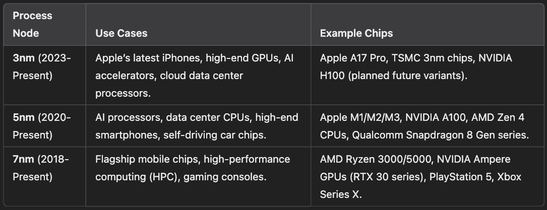
Trends in this category:
3nm technology has debuted in Apple’s A17 Pro and will expand into AI processors and HPC chips.
5nm is becoming mainstream for AI accelerators and flagship mobile SoCs.
7nm remains widely used in gaming, data centers, and high-end consumer electronics.
(B) Advanced Mid-Range Nodes (10nm - 22nm)
Who Uses It? Performance-oriented CPUs, mainstream consumer electronics, industrial automation, networking equipment.
Manufacturers: TSMC, Intel, Samsung, GlobalFoundries.
Advantages: Cost-effective balance of power efficiency and performance.

Trends in this category:
14nm and 10nm nodes are widely used in automotive and industrial applications because they provide a good balance of efficiency and cost.
Intel's transition from 14nm to 10nm was slow, causing delays in their competitiveness against AMD’s 7nm processors.
(C) Mature Nodes (28nm - 90nm)
Who Uses It? Automotive, IoT, medical devices, microcontrollers, legacy computing.
Manufacturers: TSMC, GlobalFoundries, UMC, SMIC.
Advantages: Low-cost production, excellent power efficiency, high reliability.

Trends in this category:
28nm remains a cost-effective workhorse for many applications where high performance is not a requirement.
40nm-65nm process nodes are widely used in IoT and sensor-based applications because they provide a strong balance of power efficiency and cost.
90nm chips are still relevant in older industrial equipment, where longevity and reliability matter more than raw performance.
(D) Legacy and Specialty Nodes (90nm - 250nm and beyond)
Who Uses It? Analog chips, power management ICs, smartcards, ultra-low-power sensors.
Manufacturers: TSMC, UMC, GlobalFoundries, ON Semiconductor.
Advantages: Ultra-low cost, extreme durability, longevity in the market.

Trends in this category:
Mature nodes (65nm and larger) remain dominant in power management ICs, sensors, and industrial applications.
Space and military applications use larger process nodes (e.g., 500nm to 1000nm) for radiation-hardened electronics.
3. Why Not Everything Uses 3nm?
Despite the hype around 3nm and 5nm, many industries still rely on larger process nodes due to:
Cost Efficiency: Newer nodes are very expensive to manufacture and only make sense for cutting-edge applications.
Power Requirements: Some applications (e.g., IoT, industrial automation) do not require high processing power and prioritize energy efficiency instead.
Reliability and Longevity: Older process nodes are more stable and well-tested, making them ideal for medical, automotive, and aerospace applications where long-term reliability matters.
Manufacturing Scalability: Not all fabs can produce 3nm-5nm chips; older fabs still operate at 28nm and beyond because they are sufficient for many industries.
4. The Future of Process Nodes
3nm and 2nm → Targeted at AI, cloud computing, and high-performance applications.
5nm and 7nm → Becoming more common in mainstream computing and gaming.
10nm-22nm → Expected to dominate automotive, IoT, and industrial computing for at least the next decade.
28nm+ → Will continue to be essential for cost-sensitive, power-efficient, and long-life-cycle applications.
Conclusion
Each process node has a specific niche in the semiconductor industry. While cutting-edge chips (3nm-7nm) dominate AI, smartphones, and data centers, mid-range nodes (10nm-30nm) are essential for industrial and consumer applications, and legacy nodes (45nm-180nm) still drive embedded systems, sensors, and automotive electronics. Understanding this landscape helps investors, businesses, and consumers see why smaller isn’t always better—sometimes, stability and efficiency matter more than raw computing power.
I am actively advocating market education on Bitcoin, cryptocurrencies, and web3, with the hope of empowering more people to seize this chance and benefit from these technologies, ultimately achieving genuine financial freedom. Feel free to share this article with your friends and kindly recommend this column to them.